Abstract: Total phosphorus on-line automatic analyzer has utilized C8051F020's D/A conversion, A/D conversion, UART and SPI serial communication and other enhancements. At the same time, this instrument is compact and simple in design. It is a product worthy of promotion. This article describes how to design an online analyzer and the advantages and disadvantages of the secondary product.
1. Overview The C8051F0XX series of microcontrollers is a mixed-signal system-level single-chip microcomputer newly introduced by Cygnal Corporation. This series of SCM contains CIP-51 CPU core, and its instruction system is fully compatible with MCS-51. The C8051F020 microcontroller contains 64kB of on-chip Flash program memory, 4352B of RAM, 8 I/O ports, a total of 64 I/O lines, a 12-bit A/D converter and an 8-bit A/D converter, and a Dual 12-Bit D/A Converter, Two Comparators, Five 16-Bit General Purpose Timers, Programmable Count/Timer Array with Five Capture/Compare Modules, Watchdog Timer, VDD Monitor, and Temperature Sensor section. The C8051F020 microcontroller supports dual clocks with an operating voltage range of 2.7 to 3.6V (port I/O, 5V to RST and JTAG pins). Compared with the previous 51 series microcontrollers, the C8051F020 has added many functions, and its reliability and speed have also been greatly improved.
2. Features of C8051F020 The internal functional block diagram of the C8051F020 chip is shown in Figure 1.
The C8051F020 microcontroller's core CIP-51 implements pipelined operations on the basis of keeping the CISC structure and instruction system unchanged. The device abolishes the concept of the machine cycle, and its instructions use the clock cycle as the operating unit, thus greatly improving the The speed of the instruction. When the crystal oscillator is 25MHz, the instruction execution speed of the C8051F020 can reach 25MIPS. The memory structure of the CIP-51 microcontroller is similar to that of the standard 8051. Program and data memory share the same address space, but they can be accessed using different instruction types.
The C8051F020 has eight I/O ports (64 I/O lines), including four lower ports P0 to P3 (with bit addressing) and four high ports P4 to P7 (not bit addressable ). In the C8051F020, the I/O ports can be flexibly configured through hardware switches (as shown in Figure 1). The I/O ports can also be configured to be selected by setting corresponding registers to control the crossbar switches. Functional port.
The C8051F020 has five timers/counters: T0, T1, T2, T3, and T4. Which T0, T1 and T2 consistent with the standard 8051 usage. T3 is a counter with an auto-reload function that can be used to initiate ADC data conversion, SMBus timing, and general purpose counters. The T4 can be used as a 16-bit timer for the auto-reload function, a 16-bit timer with a capture function, and a baud rate generator for the UART1. The timer/counter operation mode can be set by configuring the corresponding special function register.
Four-wire (MOSI, MISO, SCK, NSS) full-duplex serial bus can be accessed through the SPI. It can work in both master and slave modes. When the SPI of the C8051F020 operates in the master mode, the NSS is connected to the digital power supply, and when it operates in the slave mode, the device is strobed through the NSS. SPI has two full-duplex and half-duplex modes of operation. When the C8051F020 operates in the master mode of full-duplex mode, a data transfer can be initiated by writing a byte to the data register SPI0DAT. At this point, the C8051F020 will immediately shift data out on MOSI and provide a serial clock on SCK. At the same time, the slave device can also serially shift the contents of the register to the C8051F020 on the MISO line. At the end of the transfer, the SPI0CN.7 bit is set to "1". The SPI of the C8051F020 can move in/out 1 to 8 bits of data in one transfer operation to accommodate different lengths of slave devices. When the SPI is not configured as a master, it will operate as a slave.
The SMBus (System Management Bus) is a two-wire, bidirectional serial interface that complies with SMBus version 1.1 and is identical to the I2C serial bus. The C8051F020's SMBus can also work in both master and slave modes. They are started by the master device when data is exchanged.
The new C8051F020 microcontroller chip has a 9-channel, 12-bit A/D converter ADC0 and an 8-channel, 8-bit A/D converter ADC1. The channel number and channel number can be selected through register configuration when in use. Start with one of the following four A/D conversion methods.
(1) Write "1" to the AD0BUSY bit in register ADC0CN.
(2) Timer 3 overflows;
(3) Timer 2 overflows;
(4) CNVSTR has a rising edge.
The C8051F020 has two 12-bit D/A converters, DAC0 and DAC1, which can also be selected by register configuration. There are also four ways to start D/A conversion:
(1) Data is written to the high byte register of the DAC;
(2) Timer 2 overflows;
(3) Timer 3 overflows;
(4) Timer 4 overflows.
The first method is generally selected during design. When a square wave needs to be output, one of the second, third and fourth modes may be selected. In the first mode, you can also write the low byte of the DAC first, and then write the high byte to start a D/A conversion.
The new C8051F020 microcontroller develops a single pin reset as a multi-source reset including a power-on reset, brown-out reset, external pin reset, software reset, missing clock detection reset, comparator 0 reset, WDT reset, and external CNVSTR pin reset Wait. Numerous reset sources bring great benefits for the security of the system, the flexibility of operation, and the zero-power design of the system. C8051F020 perfect clock system can meet the corresponding speed under the premise of the average clock frequency can be the lowest, and multiple reset source allows the system to wake up at power-down mode.
The C8051F020 is equipped with a standard JTAG interface (IEEE1149.1) on-chip. Under the support of the host computer software, through the serial JTAG interface, the single-chip microcomputer installed on the final application system can be debugged non-intrusively, without occupying on-chip resources and full-speed on-line system. The debug system supports observation and modification of memory and registers, and supports breakpoints, watchpoints, single stepping and shutdown commands. When using the JTAG interface for debugging, all analog and digital peripherals are fully functional. In addition, the JTAG logic of the C8051F020 also provides boundary scan functionality for system testing. Through the programming control of the boundary register, we can observe and control the weak pull-up function of all device pins, SFR bus and I/O port.
In summary, the C8051F020 is a highly integrated, powerful microcontroller chip that is well-suited for applications requiring fast speeds, high reliability, extended functionality, and power savings.
3. Phosphorus on-line automatic analyzer design Phosphorus-based agents (chemicals based on organic phosphates) are widely used in industrial Water Treatment because of their good corrosion and scale inhibition performance and low pollution emissions. Due to the wide variety of phosphorus-based pharmaceuticals and the difficulty of direct measurement of organic phosphorus, the development of total phosphorus on-line analyzers can save energy and water, reduce pollution, and increase efficiency, with significant economic and social benefits. Using UV-photocatalysis and oxidation to increase the decomposition of organic phosphorus in water and monitor its decomposition water sample to achieve a quantitative analysis of the system structure shown in Figure 2.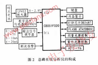
The instrument is based on C8051F020. The peripherals have expanded the data memory AT45DB081, clock chip DS1687, digital temperature sensor DS18B20, intelligent liquid crystal and keyboard, etc. They are mainly used for signal acquisition, key scan, liquid crystal display and alarm, temperature detection, industrial Standard signal output, control valve switching and various light source indications.
The data memory AT45DB081 (SPI serial interface) has a storage capacity of 8MBit and can store one year of measurement data. The clock chip DS1687 (8-bit parallel interface) can automatically update the year, month, day, hour, minute and second to complete Automatic calibration function of the instrument; digital temperature sensor DS18B20 (single-bus interface) is used to monitor the temperature of the solution to ensure the constant temperature of the liquid, speed up the chemical reaction speed, reduce the measurement period, improve the reproducibility and stability of the instrument measurement; intelligent liquid crystal (UART serial communication) and buttons are used to complete the human-machine dialogue function, forming a good man-machine interface.
The instrument uses more than 40 I/O ports, which can be used to control the switching of various valves and various light sources, keyboard input, and expansion of the DS1687. The C8051F020 has 64 I/O lines, so it can fully meet the needs. .
The use of the hardware circuit with perfect software design can achieve: keyboard operation, liquid crystal display, data acquisition and detection, data output, alarm light source control and agitator control. Figure 3 is a block diagram of the main workflow of the instrument system. When the instrument is turned on, the program first performs an initialization self-test and sets the interrupt entry address, then refreshes the LCD screen, reads the DS1687's clock signal and sends the initial density value “0.000mg/L†to the display. Open the control valve, inject the tested water sample to pre-wash the disintegration measuring cup for 1 minute, and then judge whether the key is pressed by the interrupt response. If no key is pressed, the analysis subroutine is called to complete the operation within one cycle, and the calculation result is sent to the LCD display. At the same time, it is sent to the D/A port of C8051F020 as the standard signal of the site, and the measurement result is finally stored. AT45DB081 is saved as a history record. After one cycle has been measured, the program returns to the next measurement cycle.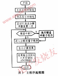
4. Concluding remarks Since the TP on-line automatic analyzer utilizes the C8051F020's D/A conversion, A/D conversion, UART and SPI serial communication and other enhanced functions, the instrument has a compact structure and simplified design. At the same time, because the total phosphorus online automatic analyzer integrates constant temperature, decomposition, measurement, and control, it greatly simplifies the chemical analysis process, improves the detection speed and stability of on-line analysis, and achieves good application results.
Automatic Descaling Water Distiller
Automatic Descaling Water Distiller,Injection Water Equipment,Steam Distillation Equipment
GuanYu Environmental Protection Equipment Corp., Ltd. , http://www.hbuvsterilizer.com